The SST protocol
Purpose
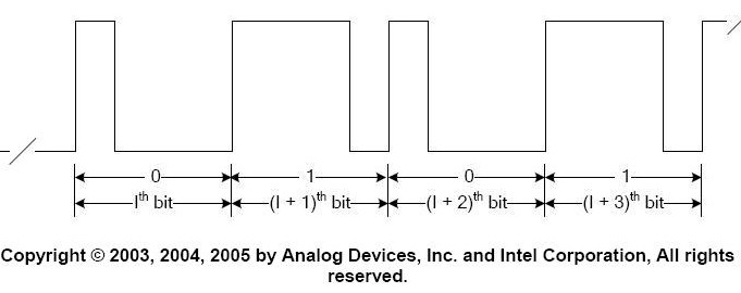
The SST protocol has unique characterestics which will be explored here. Logic 1 is defined by driving the SST line high for three quarter of period, following one quarter of period low. The logic 0 is defined by driving the SST line high for one quarter of period following driving the line low for rest of the period. It is presented in the following figure.

SST Operation
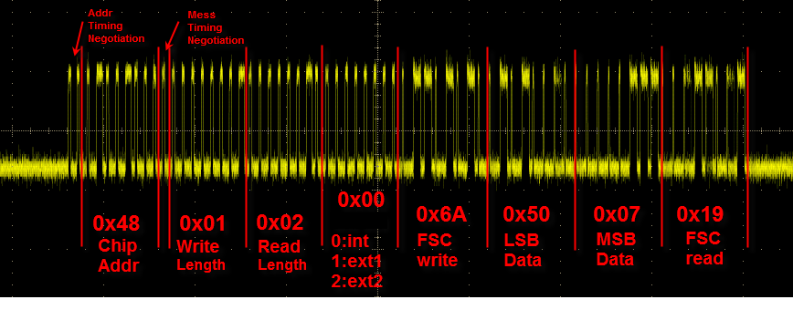
Specific sets of instructions have to be passed to the device (ADT7486A) in order to provide the right temperature. The first two zeros are called Address Timing Negotiation bits. Then the chip address will be provided following one zero, Message Timing Negotiation bit. After sending the Read Length, the Command will be provided to device to determine what type of temperature reading is required. The rest of instructions have been clearly presented on the figure.

 1.6.1
1.6.1